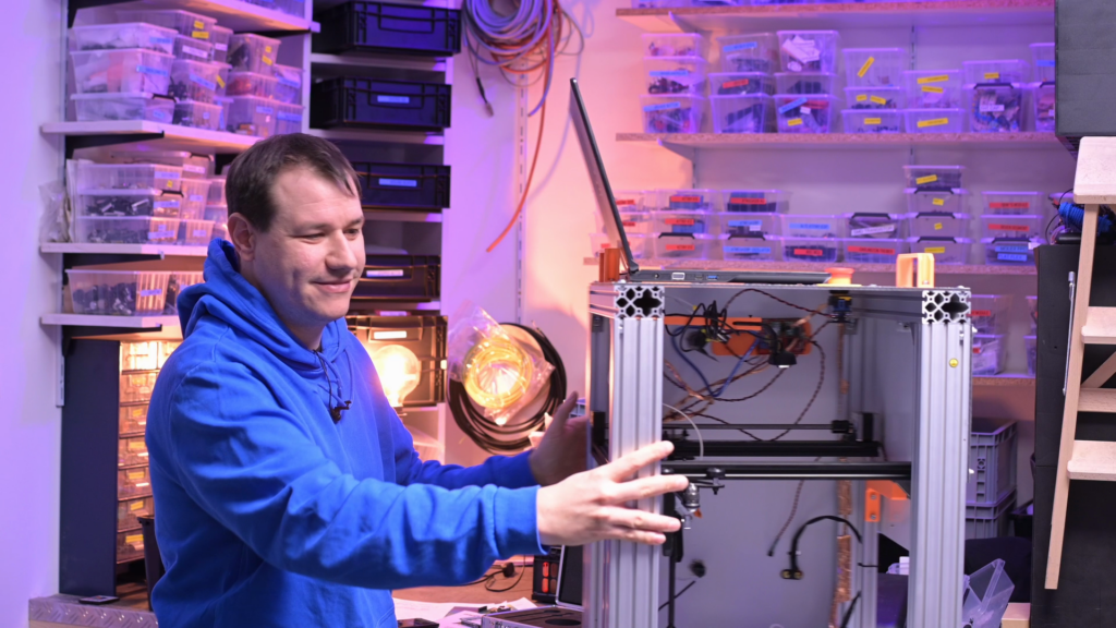
EMI (electromagnetic interference) can be a real nuisance in sensitive circuits. That might be from one device affecting another, but it can also happen when a circuit on a PCB interferes with another circuit on the same PCB (or another PCB in the same device). Engineering to prevent that entirely is really difficult and it helps a lot to be able to see where the interference is, which is why element14 Presents’ Clem Mayer converted an old 3D printer into a new EMI imager.
The goal here is to capture a “picture” of the device or PCB in question that shows the areas where EMI is highest. That picture looks like a heat map, with hot spots corresponding to areas of high EMI. But it isn’t something you can capture by snapping a photo with your Nikon. That’s where this EMI imager comes in.
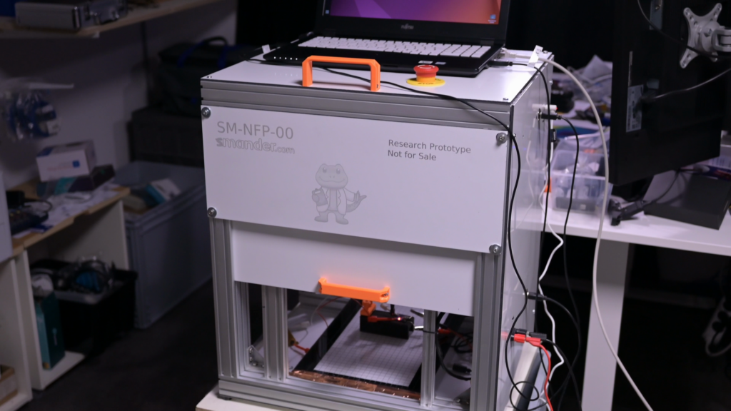
Using an old 3D printer as a motion system, Mayer’s EMI imager moves a detector back and forth across the entire area, scanning EMI levels as it goes. At many points across that area, the system records both the XY coordinates and the EMI level. After scanning, a simple script can turn that data into a 2D image.
A conventional camera mounted overhead also captures a normal photo. With the generated heat map overlaid onto the photo, the user can easily visualize the areas of the PCB or device that produce a lot of EMI.
The EMI detector is actually just an RTL-SDR module, which is affordable. It and the camera connect to a computer, which records the data. The 3D printer’s motion system operates under the control of an Arduino UNO Rev3 running Grbl 1.1, so it can run a simple G-code file that causes the toolhead (with detector) to move in a serpentine pattern across the scanning area.
If you have an old 3D printer gathering dust, this is an easy and affordable way to capture high-quality EMI images for diagnosing and improving designs.
The post An old 3D printer becomes a new EMI imager appeared first on Arduino Blog.
Read more here: https://blog.arduino.cc/2026/06/06/an-old-3d-printer-becomes-a-new-emi-imager/


